YAESU VL-1000 Quadra amplifier analysis. Power module. PA UNIT.
The VL-1000 amplifier is built with four amplifier sub-modules. Each of the four amplifier sub-modules contains 2 MRF-150 transistors. Two transistors that are identical in terms of parameters are used, the so-called "matched pair". It is possible and advisable to use 8 equal MRF-150 transistors, such as 4 matched pair, or 2 "matched quad".
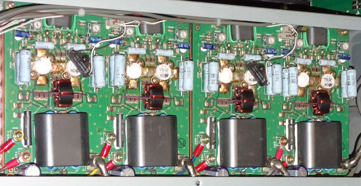
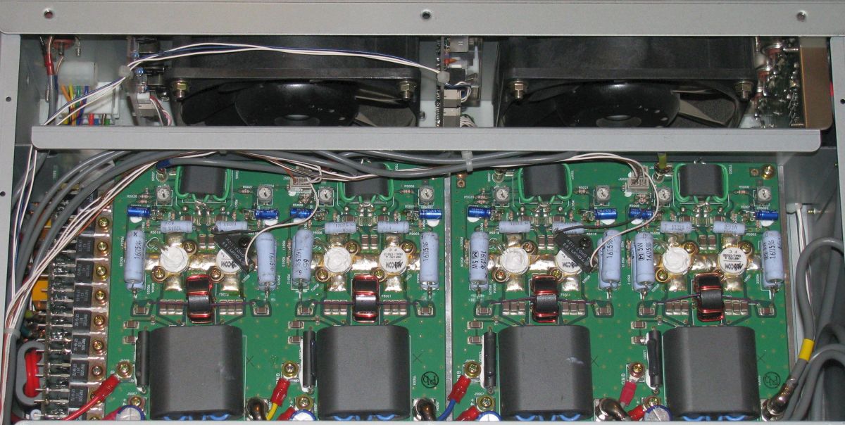
Let's see how the module of the whole amplifier looks like - PA UNIT.
Figure 1. VL-1000 PA UNIT. Click image to enlarge.
Figure 2. VL-1000 PA UNIT, second view. Click image to enlarge.
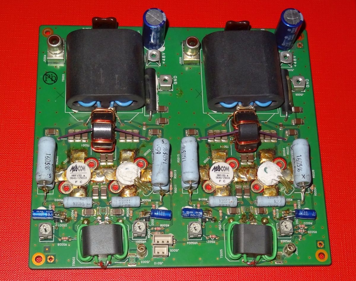
The design of the amplifier module is such that there are two amplifiers on each PCB. Let's see what the schematic of one amplifier module looks like now. Let's now see one module.
This is what the PCB of the VL-1000 amplifier module looks like, and it is a "classic" design.
Figure 3. VL-1000 PA UNIT sub-module. Click picture to enlarge.
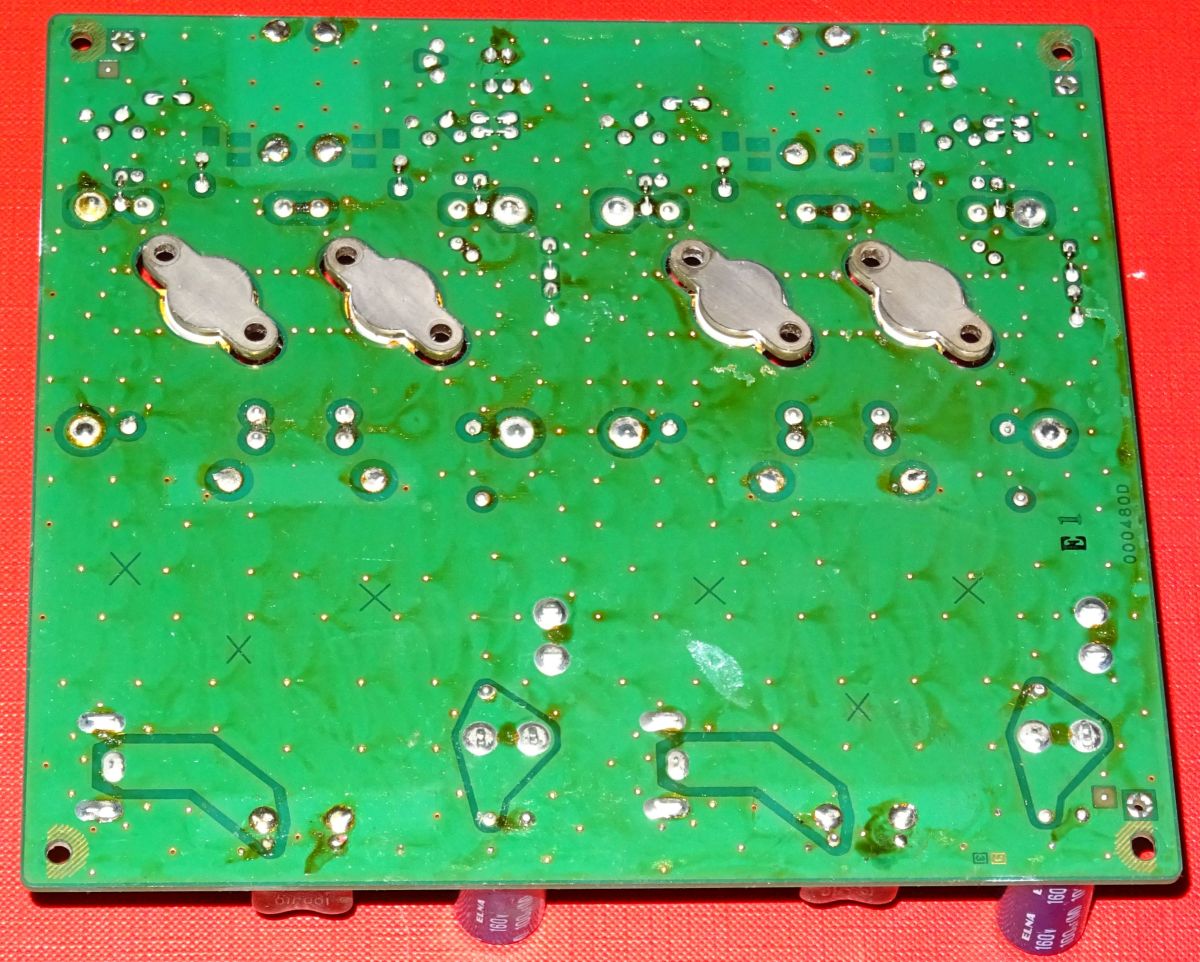
Figure 4. VL-1000 PA UNIT PCB, bottom side.

Figure 5. Block Diagram. PA boards.
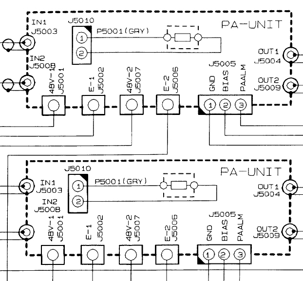
Figure 6. Block Diagram. PA UNITS interconnections.
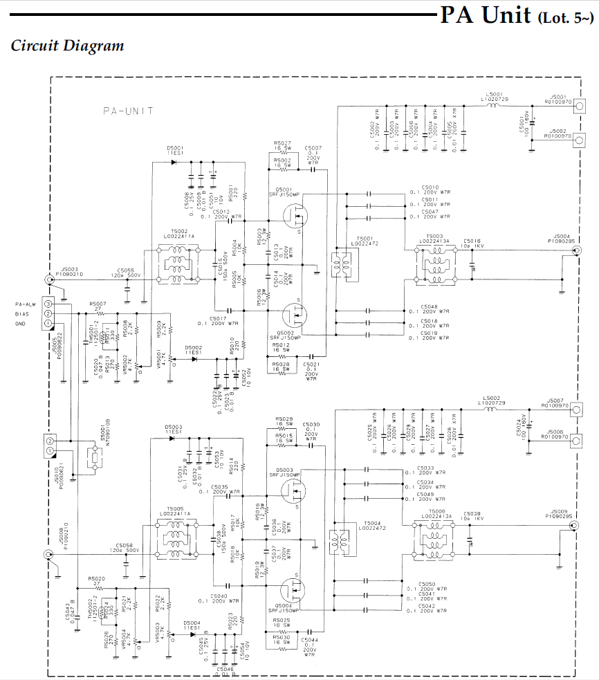
Figure 7. PA UNIT. Schematic diagram, one of four amplifier modules. Lot5+.
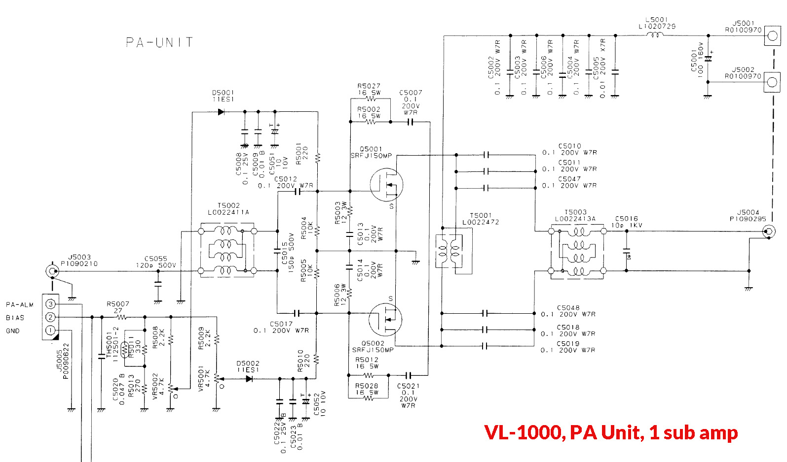
Figure 8. PA UNIT, schematic diagram, one sub-amplifier (one of four).
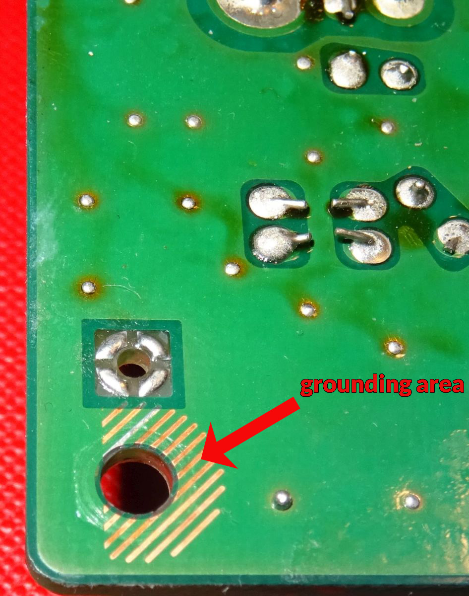
Below - PCB board of the amplifier module. Grounding problem at four (4) ground points. The board is covered with clear insulating varnish. There is no contact with the PCB ground!
Figure 9. Amplifier module grounding area. No contact with the PCB ground! The visible imprint of the brass spacer post (left - down).
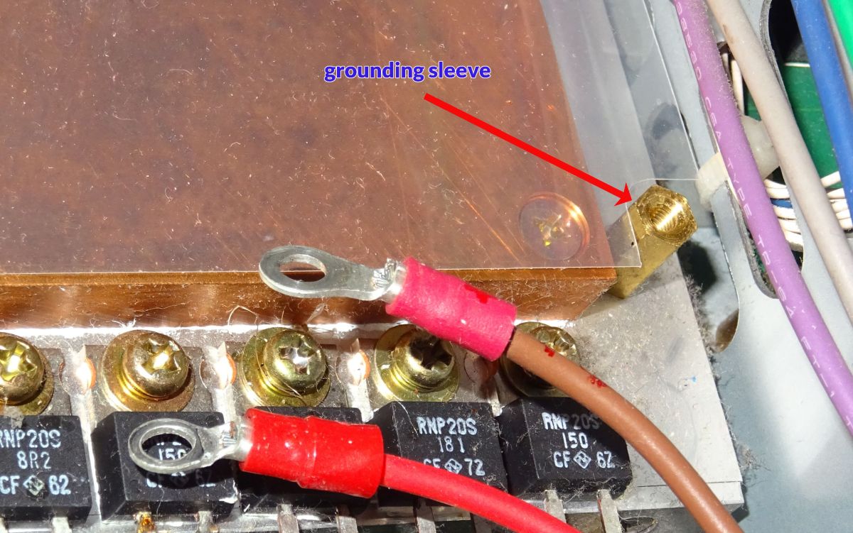
The PCB of the amplifier is attached to a dural (Al alloy) main heat sink with four (4) screws screwed into four sleeves (posts) of brass.
If one assumes that the metallization on the amplifier module's PCB board is in contact with ground through the four (4) screws attaching the amplifier board to the amplifier's main dural (Al alloy) heat sink, it makes no sense to paint the other side of the contacts with insulating varnish.
Figure 10. Grounding sleeve (post) located on main heat sink.
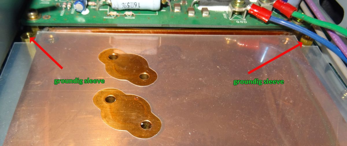
Figure 11. Grounding sleeves (spacer posts) located on main heat sink.
This is an interesting issue of how it affects the performance of the amplifier. Does it make a difference or does it not make a difference. In any case, the doubt and "ambiguity" of the design remains. Annoying issue.
... VL-1000 work will continue...










 Land Rover-ZYGI